Blog
Feb 21, 2025
Hello again
This is a distortion and wavefolding circuit built around the CD4069 IC. There are 6 gates on the chip, so its possible to build 3 of the folder/clipper circuits. These could be chained in series or used separately. One could also build a single folder and use the other gates of the IC for an oscillator. There is a quad opamp to make a mid reference voltage and to buffer the inputs of the folder for a low impedance signal to supply the circuit.
Basic idea here is like most folders as far as I know. A clipped and inverted signal is mixed with an unclipped and verted signal. The 4069 has a nice smooth clipping characteristic. By closing any one of the switches (S1-S3) the mixture of the signals changes so as to end up with only the clipped signal at the output.
Bill of Materials Revision 0
| Designators | Value | Qty | Link |
|---|---|---|---|
| BT1, BT2, BT3, BT4, BT5, BT6 | BT | 6 | Link |
| C1, C3, C5 | 105 | 3 | Link |
| C2, C4, C6 | 10uF | 3 | Link |
| R1, R2, R7, R11, R16, R19, R21, R28, R31 | 104 | 9 | Link |
| R3, R4, R14, R15, R24, R25, R26, R27 | 223 | 8 | Link |
| R5, R9, R10, R12, R13, R18, R22, R23, R30 | 473 | 9 | Link |
| R6, R17, R29 | 472 | 3 | Link |
| R8, R20, R32 | 102 | 3 | Link |
| RV1, RV2, RV3 | POT | 3 | Link |
| SW1, SW2, SW3 | SW_SPST | 3 | Link |
| U1 | CD4069 | 1 | Link |
| U3 | TL074 | 1 | Link |
send me an email if you build it! if you find some issues please let me know as well.
mill dot lorre at g mail dot com
Love,
-Will
Apr 29, 2024
Schematics updated 06/07/24
Ok, coming back around to clear the cobwebs out of this dusty old blog once again. I haven’t been good about keeping up with this, and I hope for that to change…
My new aim for this blog is to be posting circuits that will work well on a single 9v power supply. Great for DIY of course! Noise circuits to create noise projects with. With a CC BY-NC-SA License. Non-commercial use only. I plan to sell PCBs of some designs in the future, but for now will just try to consistently post schematics for all you brave electronics DIYers out there.
These designs will use jellybean parts, the E6 series of preferred numbers for resistors and capacitors, simple as possible.
First up! Cycling24
This design is another riff on the same basic idea Ive been orbiting for years. Cycling shift registers... In this case a 24 bit shift register. This can be used as an LFO or tone source oscillator. Try sending something into the data input.
Falstad simulation to test resistor combinations
Also included in the falstad is the idea to use a square wave osillator at the data input to get some interference pattern propigation.
Check the REV1 edits!
Beginning with the Data input jack on the upper left hand corner of the page is a comparator which compares the signal on the non-inverting input with 4.5v made by the resistor divider (R8,R9). Change this if you like to have the comparator point somewhere else. Below the comparator is an LED driver around Q1. The output of the comparator goes into the CD4046 Phase locked loop chip. Pins 3,14 and 2 interface with an XOR gate on the chip. This XOR gate is called “Phase Comp I” in the CD4046 datasheet. Pin 3 of the CD4046 is the data loop from the end of the register. Output of the XOR gate feeds the data input to the shift register chain (U3,U4,U5).
Q2 and Q3 make a differential amp used to sink current from the CD4046, changing the pitch of the internal oscillator. Note the potentometer on the left side of the diff amp is clockwise to gnd as that side is inverting.
SW1 and associated components make a short positive going pulse by high-passing the edge of the switch press and clipping any negative swing with the diode. This is mixed with the Clear input banana jack.
The long chain of resistors is a mixer mixing all of the bit outputs from the shift register chain. I’ve linked the circuit in Falstad’s excellent interactive analog circuit simulator. There you can test different resistor values for the mixer. The values used in this design are the E6 values starting at 470k going down to 6.8k and then back up the series. This gives a clipped-sine type mixture a la the digital sine wave generator from the CMOS cookbook.
This design can doubly function as a type of sequencer. You could add a way to loop the register at different lengths like a rotary switch or patch points. And also add jacks to the outputs of the registers which you might want to loop from or use as gate signals.
The PDF features art by Fiona from I think 2017. I hope its ok I’m using your art as part of this, Fiona. The images were made as repeating background-image tiles for a website.
The component values in the schematic and materials list use this convention: 103 = 10 + 000 = 10k. 474 = 47 + 0000 = 470k.
If you come across something that is almost certainly a bug, please let me know via my contact form. I will try to answer build questions and troubleshooting messages but I can’t promise to be super quick to respond.
Bill of Materials Revision 1
| Designators | Value | Qty | Link |
|---|---|---|---|
| BT1, BT2, BT3, BT4, BT5 | Banana Jack | 5 | Link |
| C1, C3 | 103 | 2 | Link |
| C2 | 102 | 1 | Link |
| C4, C5 | 104 | 2 | Link |
| D1 | LED | 1 | Link |
| D3 | 1n4148 | 1 | Link |
| Q1, Q2, Q3 | 2N3904 | 3 | Link |
| R1, R4, R8, R9, R25, R30, R31, R34, R44, R45, R47, R48 | 103 | 12 | Link |
| R2, R7, R17, R18, R26, R39, R49, R51 | 104 | 8 | Link |
| R3, R19, R21, R36, R50, R53 | 473 | 6 | Link |
| R5, R10, R13, R37, R46, R52 | 102 | 6 | Link |
| R6, R15 | 222 | 2 | Link |
| R11, R43 | 474 | 2 | Link |
| R12, R42 | 334 | 2 | Link |
| R14, R28, R41, R54 | 224 | 4 | Link |
| R16, R40 | 154 | 2 | Link |
| R20, R38 | 683 | 2 | Link |
| R22, R35 | 333 | 2 | Link |
| R23, R33 | 223 | 2 | Link |
| R24, R32 | 153 | 2 | Link |
| R27, R29 | 682 | 2 | Link |
| RV1 | 100K Linear Pot | 1 | Link |
| SW1 | SPST Pushbutton | 1 | Link |
| U1 | TL064 | 1 | Link |
| U2 | CD4046 | 1 | Link |
| U3, U4, U5 | CD4015 | 3 | Link |
Jun 2, 2022
Site style changes. I have replaced the gradients with solid colors. No more gradients, my GF says its too soon try and bring those back, just tacky. I see what she means. Also so big a style jump from my previous site style, not cool. I get it. Some general styling issues with padding and spacing things are also now better.
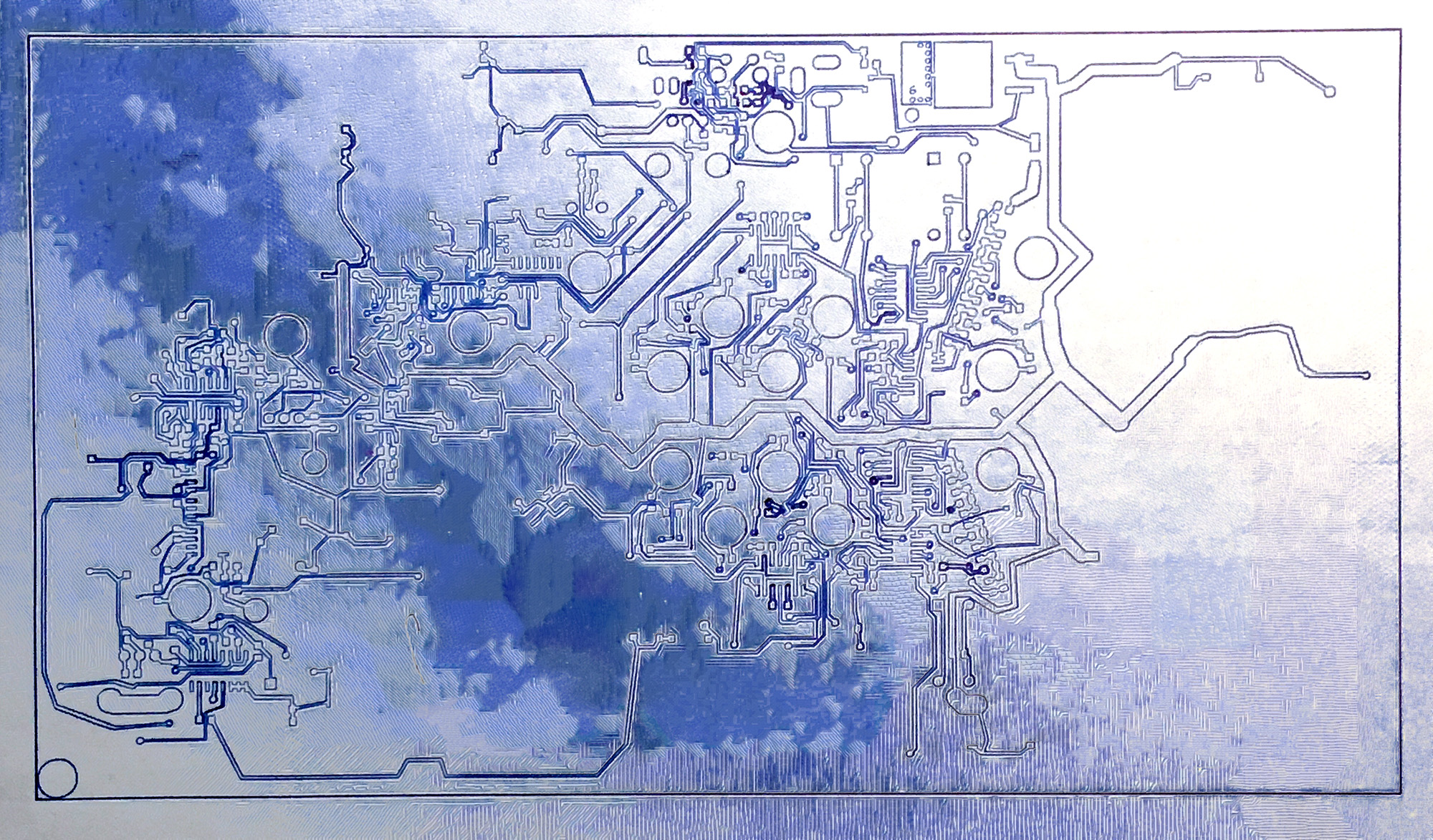
Double Knot v3 cases are in PA undergoing silk-screening. Circuit boards and most of the parts are here getting ready for pick-and-placing. A few little part hiccups but they should be in the machines populating soon! Finishing up the user manual and will be burning a silkscreen to print boxes soon. Here is a pen plot of some traces from the circuit board artwork "cultured" in Photoshop.